 US / English
Wafer Foundry Services
Lab-to-Fab Partner
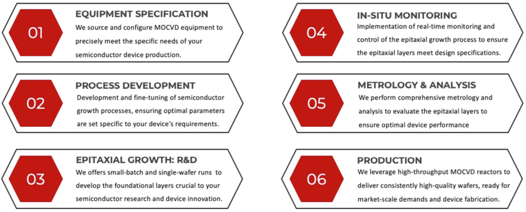
Alliance MOCVD is committed to providing comprehensive solutions—from equipment to process development and metrology to production—that empower our customers to transform ideas into market-ready products.
Process Development
From concept to final product, our vertically integrated process ensures efficiency and consistency at every stage.
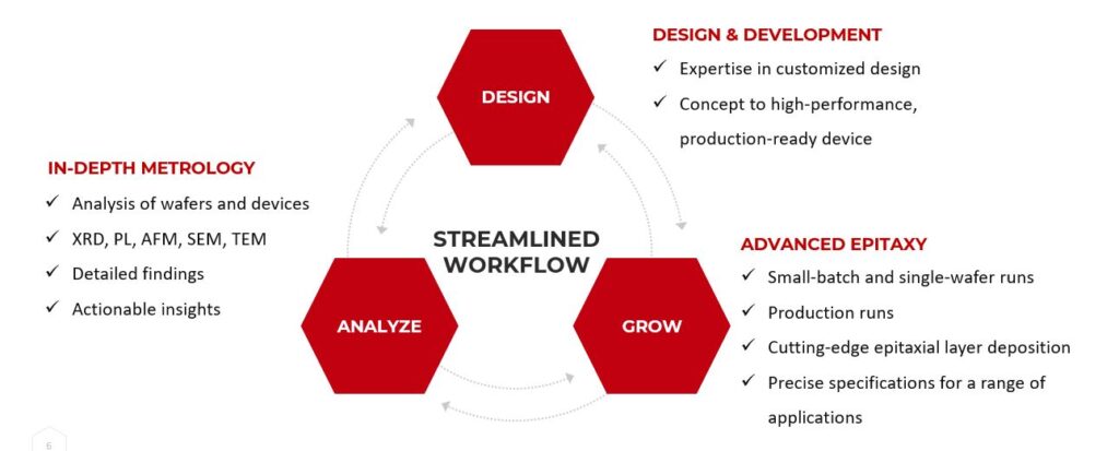
At Alliance MOCVD, our process development services are at the core of what makes us unique. Our expert team specializes in advanced Arsenic Phosphide (AsP) and Gallium Nitride (GaN) epitaxy, crafting high-precision structures for a wide range of electronic and photonic applications.
Whether you are looking to improve the poor performance of your current basic recipe or are in need of assistance developing a new process, our highly skilled process engineers are here to help.
Structure Specialization
Development and optimization of MOCVD processes with a focus on GaN and AsP.
Creation of tailored processes that enhance the material quality, device efficiency, and yield, addressing the specific requirements of each client’s project.
GaAs
High Electron Mobility Transistors (HEMTs) and Diodes
InGaP/AlGaP
Heterojunction Bipolar Transistors (HBTs)

GaAs and InP
Based Optoelectronic Device Structures (LEDs, Laser Diodes)

GaN/Sapphire
Optoelectronic and Electronic Structures
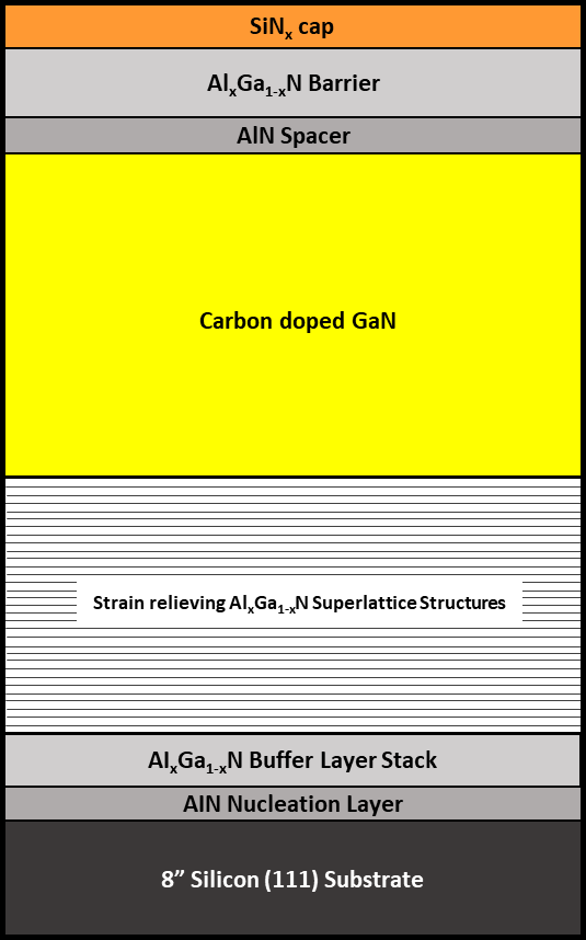
GaN/Si
Power and RF Structures
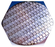
Wafer Services
We leverage high-throughput MOCVD reactors to deliver consistently high-quality wafers, ready for market-scale demands and device fabrication. Our wafer services are designed to maximize epitaxy uniformity and yield, accommodating a variety of wafer sizes.
We offer small-batch and single-wafer runs to develop the foundational layers crucial to your semiconductor research and device innovation.
Real-time monitoring and control of the epitaxial growth process is used to ensure the epitaxial layers meet design specifications.
Metrology & Analysis
At Alliance MOCVD, we ensure the highest quality of your semiconductor projects through our expert metrology services. Each analysis concludes with an in-depth report, offering detailed findings and actionable insights to enhance your product’s performance and reliability.
Available Services:
- X-ray Diffraction (XRD)
- Atomic Force Microscopy (AFM)
- Photoluminescence (PL)
- Hall Measurement
- Scanning Electron Microscopy (SEM)
- Transmission Electron Microscopy (TEM)
Advanced Defect Analysis
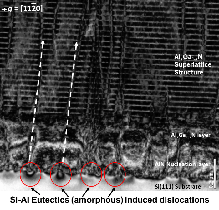
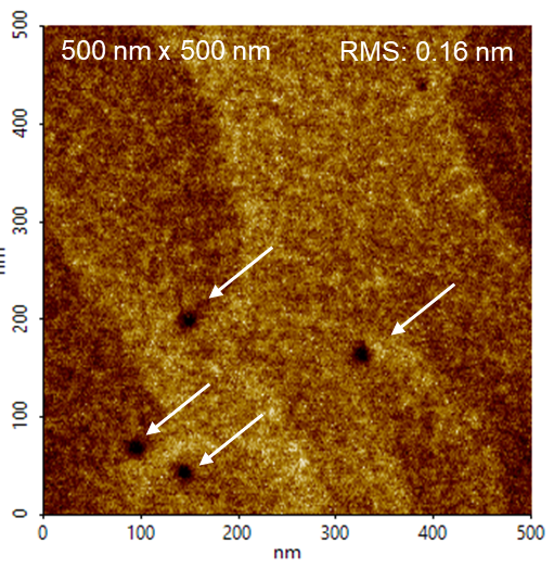
Advanced defect analysis by a combination of AFM and TEM to trace the origin of surface defects/traps affecting the performance reliability of a GaN/Si HEMT structure.
Bright-field cross-sectional TEM image of HEMT structure bottom comprising AlN nucleation layer and part of AlxGa1-xN buffer stack and the surface AFM with defects originated from bottom.
These cutting-edge techniques provide deep insights into material properties, enabling us to refine our processes continually and deliver products that exceed expectations.
End-to-end Solution Partner
Alliance MOCVD stands as a vertically integrated end-to-end solution provider in the semiconductor industry, streamlining the journey from concept to commercialization.
With expertise spanning equipment design, process development, advanced metrology, and wafer production, we offer a cohesive suite of services under one roof.
Our holistic approach ensures seamless project progression, superior quality, and accelerated innovation for our clients, positioning Alliance MOCVD as the partner of choice for leading-edge semiconductor solutions.
Let’s Innovate Together
Whether you’re looking to bring a new semiconductor device to life or seeking support for legacy MOCVD equipment, Alliance MOCVD is your go-to partner. Together, we can drive the future of technology, transforming challenges into opportunities for growth and innovation.